A-Circuit Tutorial


THE GRAPHICAL INTERFACE
 

The purpose of the interface  is to let the user:

When drawing the circuit, the user is allowed to add gates to the circuit, to connect gates to each other with wires and to delete  gates and wires. Figure 1 shows a snapshot of the interface. The circuit is displayed in the Circuit Window, while the ToolBox Window contains buttons for each of the above operations.


EXAMPLE
 

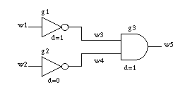
Let's follow the steps to draw the following circuit:

Figure 2

Figure 2

  1. Run the interface by typing on the command line:
    1.  
      % /usr/local/bin/ACircuit


    Two windows will appear on the screen:

    1. Circuit Window
    2. ToolBox Window

     
  2. Draw a gate.

  3. First, using the mouse, select the type of gate you want to draw from the buttons on the ToolBox Window.
    Next, click inside the Circuit Window on the position where you want the gate to appear.
    A dialog box will appear requesting:
      (1) the number of input pins of the gate (if it allows different number of input pins), and
      (2) the delay associated to the gate.
    At this point, the gate will be given an automatically generated name and will be shown in the Circuit Window.

    To draw NOT gate g1 from figure 2 perform the following actions:

    1. Click on the Not button of the ToolBox Window.
    2. Click inside the Circuit Window at the position where you want the gate to appear.
    3. Enter delay=1 (note: the number of pins is not requested because NOT gates have only one input pin).
    Similarly, draw gates g2 and g3.
     
     
  4. Connect gates.

  5. To connect the output of a gate to the input of another gate: first click on the Wire button in the ToolBox Window, next click on the output pin of the first gate in the CircuitWindow, finally click on the input pin of the second gate in the same window. Then, the wire connecting those gates appears in the Circuit Window.

    Let's draw the wire connecting the output of g1 and the topmost input pin of g3 from figure 2 Perform the following actions:

    1. Click on the Wire button of the ToolBox Window.
    2. Click, inside the CircuitWindow, on the output pin of g1.
    3. Click on the topmost input pin of g3.
    Similarly, connect g2 with g3.

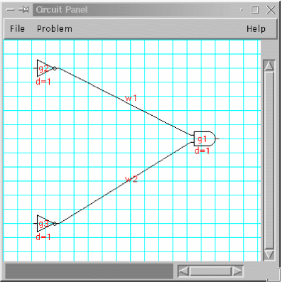
    Now that the circuit's drawing is complete (see its picture here), we are ready to select a problem to solve.


  1. SIMULATING THE CIRCUIT

  2. In order to select the simulation problem, click the Simulation option of the Problem menu in the CircuitWindow.

    The simulation of the circuit will be performed for the time interval from 0 to an upper bound called "lasttime".
    You will be requested to enter the following information:

    Once all data have been entered, the simulation is computed and the results are displayed as follows:


    Click here to see sample snapshots of the CircuitWindow and of the AnalyzerWindow for the above circuit.


  3. ABDUCING INPUT SIGNALS OF THE CIRCUIT

  4. To select the abduction problem, click the Abduction option of the Problem menu in the CircuitWindow.

    Currently, we have only the static case of abduction of input signals available. This means that once a signal value is applied to an input wire W at time T, then no other values can be applied to this input wire in a future moment of time.

    The system will require that you enter:

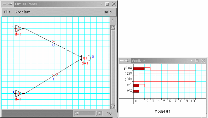
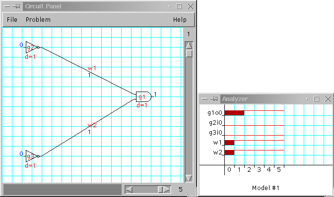
    Given the above data, the program abduces the input signal values for the circuit and the solution is presented in the following way:

    Since it is possible to produce the desired output from different combinations of input signal values, the program may generate multiple solutions. If this is the case, by dragging the vertical scrollbar located on the right side of the CircuitWindow you can browse through the different solutions.

    Click here to see a snapshot of the CircuitWindow and the AnalyzerWindow for the above circuit when


  5. GLITCH-DETECTION

  6. The glitch-detection problem is selected by clicking the Glitch-detection option of the Problem menu in the CircuitWindow.

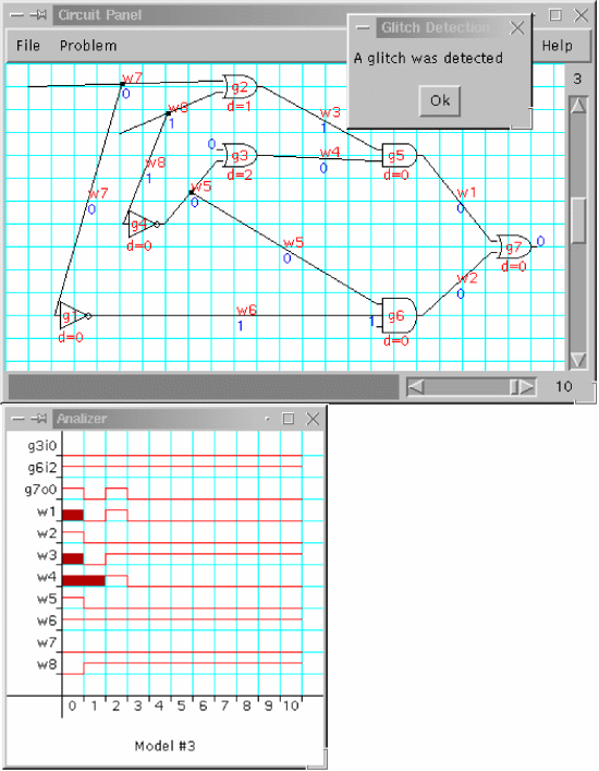
    As in the simulation case, you are requested to enter the value of "lasttime". Then, the program checks if glitches can appear in the circuit outputs under single transitions of the input values. A dialog box is displayed showing whether the circuit is glitch free or if a glitch was detected. In the last case, the occurrence of a glitch on an output can be seen in the AnalyzerWindow.

    If glitches occur for different transitions on the inputs, it is possible to browse through the situations, in which a glitch appears, by dragging the vertical scrollbar located on the right side of the CircuitWindow.

    Here are some snapshots showing the detection of a glitch in a circuit.


  7. MAX DELAY OF CIRCUIT

  8. The topological critical delay of a circuit corresponds to the maximum delay it would take for signals to stabilize at output gates. Maximum delay of a circuit is the computation of the topological critical delay of the circuit. Option Max delay is available on the Problem menu in the CircuitWindow.

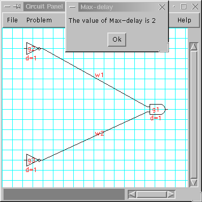
    Once this option is chosen, the system will compute the maximum delay of the circuit and the value computed will be then displayed on a dialog box (see an example here.)